
AI has entered a phase where the limits are no longer set by algorithms or transistor counts but by energy and speed.
For years, the industry relied on a simple strategy: Deploy more Graphics Processing Units (GPUs). That approach is now colliding with physics. Datacenters push megawatts of power, airborne and orbital systems cannot dissipate power, and edge computing devices live under strict energy consumption. Scaling electronic computing alone is no longer feasible.
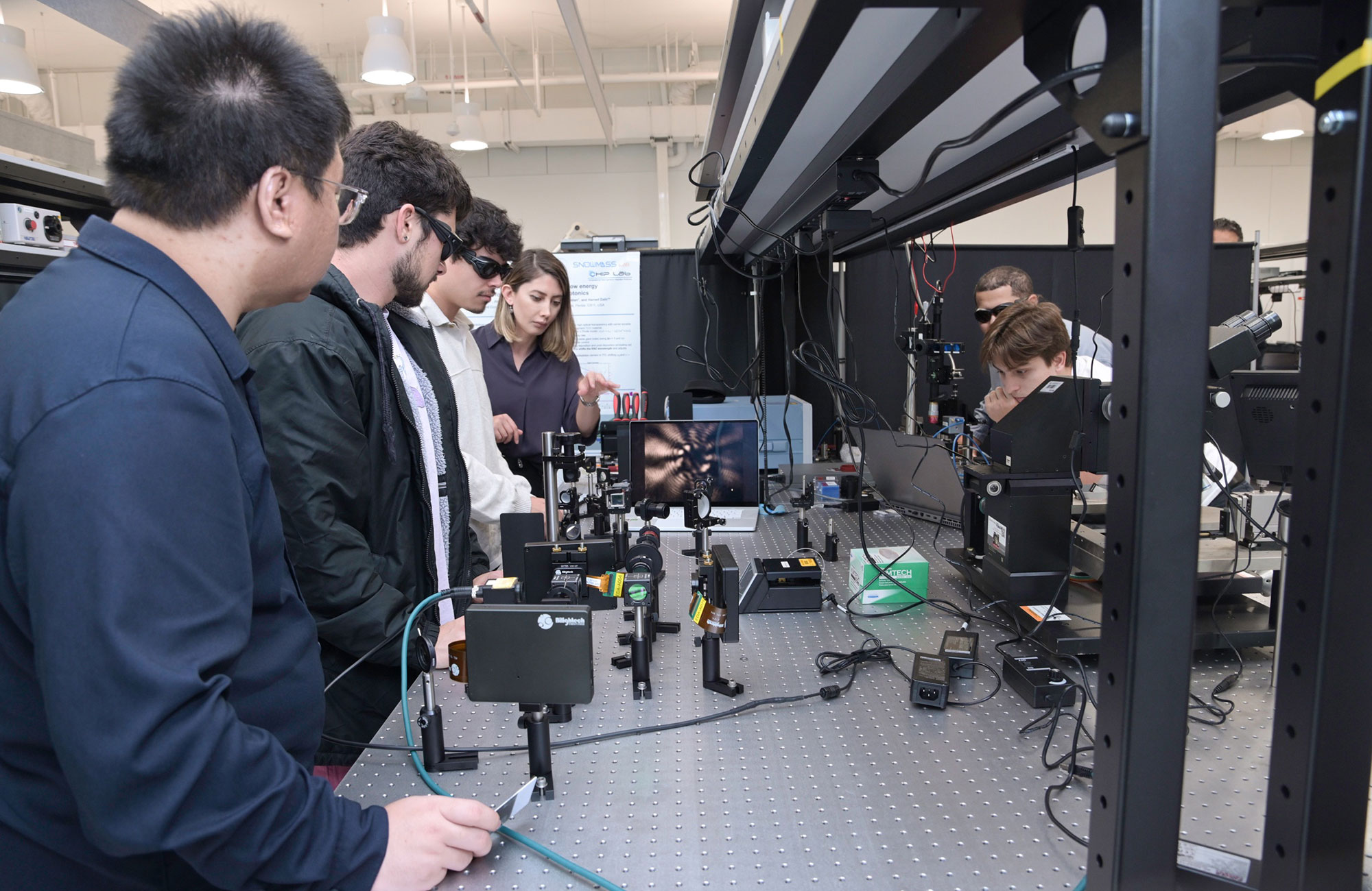
Researchers at the University of Florida are seeking a new direction. In work published in Photonics Research, UF engineers demonstrate a hybrid photonic–electronic neural network that shifts one of the most energy-intensive stages of AI — feature extraction — into light itself. The result is dramatic: 6.5 times faster training and nearly 1,000 times higher energy efficiency than an all-electronic baseline.
“AI acceleration is becoming an energy problem as much as a computing problem,” said Elham Heidari, Ph.D., assistant professor in the UF Department of Electrical and Computer Engineering (ECE) and an American Chemical Society Photonics Rising Star. “Our results show a practical path where light performs the front-end neural processing, so electronics don’t have to carry the entire load.”
“Start with photons, end with electrons — that’s how AI scales with physics, not power.”
– Elham Heidari, Ph.D., assistant professor in the UF Department of Electrical and Computer Engineering
A neural network that thinks in light
Architecture challenges a long-standing assumption that meaningful computation must wait until after digitization. Instead, the UF system performs the front-end transformations in the optical domain.
A Fourier-domain wavefront processor, shaped by programmable phase control, performs massively parallel feature extraction in light long before the signal reaches electronics. This inversion of computational order plays to the natural strengths of each domain. Photons perform large parallel transforms with almost no energy. Electrons excel at programmable logic and compact memory.
Together they form a hybrid engine that uses physics not power to unlock scale.
As AI models grow, it is these front-end transformations that dominate energy consumption. By executing them in optics, UF’s approach sidesteps the thermal and power crises that define next-generation accelerators.
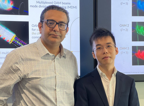
“The future of AI accelerators is hybrid,” said Jiachi Ye, UF ECE alumnus and first author of the paper. “Photons handle the high-throughput parallelism, and electrons perform the precise logic. That’s how you scale performance without scaling heat or power.”
The road ahead: From free-space prototypes to multi-GHz integrated photonics
The present demonstration uses a 60 Hz liquid-crystal spatial light modulator (SLM). Its speed ceiling has nothing to do with the architecture and everything to do with the component. Replacing that SLM with a photonic-integrated circuit built around indium–tin-oxide (ITO) modulators moves the design from the world of human-visible updates to radio-frequency operation.
“Jumping from 60 Hz to tens of gigabits per second is not an upgrade but a new physics regime, what the free-space SLM accomplishes in a full second, an ITO photonic chip completes in a couple of nanoseconds,” said Tongyao Wu and Abdulaziz Bazammul, both current ECE graduate students.
Vertical integration: Photons and electrons stop cooperating and start unifying
The long-term vision pushes beyond even planar photonic integration. UF’s roadmap leads toward true three-dimensional heterogeneous integration a stack where multilayer photonic computing planes sit directly beneath sub-10 nm electronic logic.
Through vertical bonding and chip-scale interconnects, the photonic and electronic domains stop being separate technologies and become a single computational system.
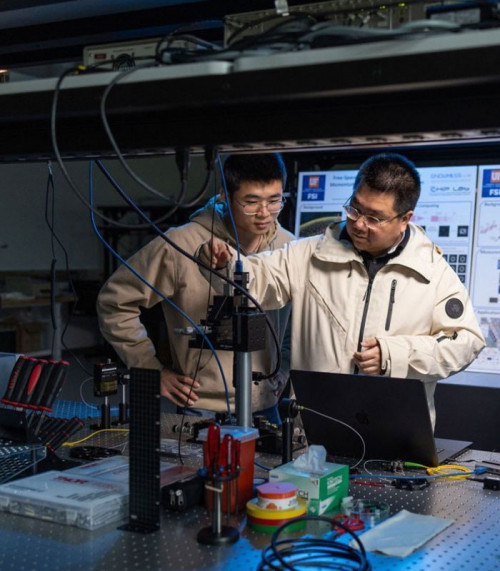
“We have been beginning to work with a major foundry on 7 nm nodes, and shortly we will move to 5 nm, depending on what the system demands,” said Hamed Dalir, Ph.D., ECE associate professor and director of UF’s Center for Heterogeneous Integration and Photonics (CHIP) Lab.
“Our goal is to have the first vertically integrated photonic–electronic prototype ready as early as 2027, showing this architecture not just as an idea, but as a deployable accelerator capable of setting new limits in speed, efficiency, and density,” said Dalir.